The iPhone 4G seems to have been spotted in the wild, and as far as knock-offs go, this one looks quite authentic, with severalparties finding the evidence credible and going so far as to say “it is incredibly likely” the new iPhone will look like the device in the pictures. The device seems remarkably similar to the phone in the images posted on February 20th by a Chinese Tweep, who claimed his photos were taken at a Chinese “testbed” for Apple
.Found in an iPhone 3G case in a San Jose watering hole, the device has been observed to have a front-facing camera, a higher-res back-facing camera with flash, an 80GB hard drive, a 960x640 resolution screen, MicroSIM support, a “radio transparent” ceramic enclosure, and a “decidely new OS” which apparently does not boot anymore. Some seem to think this is device is still on a testbed frame, and that the final-release device will not have such visible and “un-Apple-like" seams on the side. The new owner is looking to sell the device. Find some more pictures in the gallery below.
Images courtesy: Engadget and Weiphone sources : digit
Back in 2001, to give people a new, quicker way to find images, we launched Image Search. When you do a search for [eiffel tower] you'll find an array of images of the tower in the daytime, in black and white, at sunset and more. With Similar Images, which recently graduated from Google Labs, you can click "Find similar images" to narrow your search to, say, pictures of the Eiffel Tower lit up at night. Today, we've launched an experimental feature in Labs called Google Image Swirl, which builds on new computer vision research to cluster similar images into representative groups in a fun, exploratory interface.For example, if you search on Image Swirl for [washington], you'll see 12 image thumbnails including President Washington, the Washington Monument, a map of Washington D.C. and the Capitol Building:
Once you find the group of images you're interested in, you can click on the thumbnail and a cluster of images will "swirl" into view. For example, here's what you'll see if you click the image of the Washington Monument:
You can then further explore additional sub-groups within any cluster. The interface may look familiar to those of you who have tried Google's Wonder Wheel available in the Search Options panel, which enables you to explore related search queries.
Image Swirl expands on technologies developed for Similar Images and Picasa Face Recognition to discern how images should be grouped together and build hierarchies out of these groups. Each thumbnail on the initial results page represents an algorithmically-determined representative group of images with similar appearance and meaning. These aren't just the most relevant images — they are the most relevant groups of images.
Image Swirl currently works for more than 200,000 queries and we plan to include more queries in the future. Available queries will auto-complete as you start to type in the search box, similar to Google Suggest.
You can try out Google Image Swirl in Google Labs today. The feature is experimental and the underlying technology is a work in progress.
In case you hadn’t noticed already, here is a heads up: Google launched another feature in quick succession, and this time it is “Drag and Drop Attachments” for Gmail.
A feature that all Gmail users can be happy about is unfortunately limited to Google Chrome and Mozilla Firefox 3.6 users for now. However, Google does promise that they will “enable this for other browsers as soon as they support this feature”.
If you are someone who regularly attaches things to their mails and use Gmail, then don’t wait for the functionality to come to other browsers! Switch now!
In related news, Google also introduced another interesting feature, a long required functionality that allows users to send a Google Calendar Invitation (in other words, create Calendar events) directly from their Gmail.
This is how it appears:
You can then customize the invitation, (choose a time etc.), preview it, and then insert it into the email. Once you send the mail, the invitation will be added to your calendar, as well as your friends’.
The whole world is looking for alternatives to silicon-based computational and storage devices. As you squeeze circuits together in a smaller space, you are approaching the theoretical limits of scale and heat dissipation envisioned decades ago, causing the circuits to melt after a certain tiny size. Manufacturing silicon transistors on such a small scale is also unbelievably complex and expensive, and has its own limitations, where the size of the circuits designed become smaller than the wavelength of light used to create them. Newer manufacturing technologies (electron beam lithography, micro lasers) are being developed that can circumvent this second problem, but the resultant circuits, though incredibly minute, will still be affected by heat unless they can dissipate it fast enough. Researchers at HP Labs however, believe that the answer lies elsewhere, ironically in a type of circuit element that was proposed way back in 1971 by Leon O. Chua, an electrical engineer at the University of California, Berkeley.
Deemed unfeasible, memristors, or memory resistors as a concept in the 70s relied on magnetic flux. But in 2008, researchers at HP Labs realised that memristors could be “read and written using applied voltages”, and didn’t require magnetic flux quite as much as thought. Now, those same researchers at HP Labs have developed working memory resistors that function at the same speeds as today’s conventional silicon transistors, and say the technology will progress much faster than Moore's law previously dictated.
Why they are better than silicon transistors
One of the things that make memristors so interesting is that they can simultaneously “perform a full set of logic operations at the same time as they function as non-volatile memory”. This will enable designers to design circuits built out of memristors that operate both as memory and processing units, thereby replacing the need for specialized units and the time-consuming required communication between them. They are also simpler to manufacture than silicon transistors, much more energy-efficient (see why below) and virtually immune to radiation disruption.
Memristors will also free designers to work in three dimensions, and to be able to “stack thousands of switches on top of one another in a high-rise fashion, permitting a new class of ultra-dense computing devices even after two-dimensional scaling reaches fundamental limits.” HP said in an official statement, "In five years, such chips could be used to create handheld devices that offer ten times greater embedded memory than exists today or to power supercomputers that allow work like movie rendering and genomic research to be done dramatically faster than Moore's Law suggests is possible."
Stan Williams, a physicist at HP, says “memristor technology really has the capacity to continue scaling for a very long time, and that’s really a big deal.” Today’s conventional silicon transistor technology is based on minimum feature sizes of 30 to 40 nanometers, and by contrast, working 3-nanometer memristors have been designed which can switch on and off in about a nanosecond, or a billionth of a second, much faster than ordinary silicon transistors.
Currently, memristors can store 100 gigabits on a single die in one square centimeter, much more than the 16 gigabits for a single flash chip. In the future, HP thinks they can get that up to a terabit or more per centimeter, meaning almost 20 gigabytes a square centimetre, outstripping projections of future flash memory device capacities by almost a factor of two.
Another amazing feature of memristors comes from their scalability. As you know, that as silicon transistors get smaller, they face many problems, including heat and complexity issues. The exact opposite is true of memristors. The smaller they get, they stronger their memristance effect, allowing them to scaled down for a long time to come, only limited by our nano-manufacturing capabilities.
Check out a short video below of Dr. Stan Williams from HP Labs explaining the potential of memristors:
How they work
Electronic circuit theory was traditionally based on three components: the resistor, the capacitor, and the inductor. The memristor is now considered the fourth. There are four fundamental circuit variables: electric current, voltage, charge, and magnetic flux. Each of the three above mentioned electronic components managed to link two out of four circuit variables - allowing for calculations to be made - where resistors relate current to voltage, capacitors relate voltage to charge, and inductors relate current to magnetic flux. But, what was missing was a way to relate charge to magnetic flux. This where the memristor comes in.
According to researchers at HP, "The fact that the magnetic field does not play an explicit role in the mechanism of memristance is one possible reason why the phenomenon has been hidden for so long; those interested in memristive devices were searching in the wrong places." It has now been realised that relating magnetic flux to charge is based on variable resistance as a function of the charge passed through it.
The technology uses electrical currents to move atoms within an ultrathin film of titanium dioxide, a part of which compound is 'doped' to have some missing oxygen atoms. It is these holes, or defects in the crystal that allow an electric current to pass through titanium dioxide. The more holes, the lower the resistance. This is how resistance states can be created, based on the movement of oxygen atoms, detecting a single atom moving a single nanometer. Each movement can be read as a change in the resistance of the material, which persists even after the current is switched off, making extremely energy-efficient devices when compare to silicon transistors, which require a constant electrical current (or lack thereof) to maintain its state.
HP's working memristors are capable of adopting either high or low-resistance states, which can be considered as equal to the 'on' or 'off' states of conventional silicon transistors, where '1' is the presence of the electron charge, and '0' is the lack of charge. A certain positive voltage will flip the memristor to its high-resistance state, while a negative voltage of the same magnitude will flip it to its low-resistance state. These states are stable, and therefore are can allow the memristor to work as non-volatile memory, not requiring the electrical current to maintain the state.
The memristor approach that is very different from a type of storage developed by IBM, Intel and other companies, called “phase-change memory”. In phase-change memory, heat changes the phase or state of a glassy material from an amorphous to a crystalline state, which requires time and consumes lots of power, making it energy inefficient and slow.
Because of their non-volatile nature, memristor-based systems can also be used to produce analog computing systems, functioning more like biological brains, as they work similarly to biological synapses. This is considered by many to be the holy-grail of electronic technology.
A new kind of logic
Most silicon transistors perform a full set of logic operations using a combination of NAND (not-and) gates. Previously, it was thought that memristors will not be able to perform a full set of logic operations. But, it has now been found that a memristor can also be made to transfer its state to other memristors, therefore producing devices that can reprogram themselves in a manner that depends on the evaluation of other logic operations. Memristors can hence use NAND gates for logical operations, but in a new way, with a combination of three memristors using a logical operation called "material implication", where for Boolean states p and q, a material implication is "p implies q", and if p is true, then q must also be.
It is also possible to build an IMP logic gate by using two memristors and combining them with a standard resistor. When you add a further memristor, it can act like a false operation (it always returns false), to deliver a complete set of logic operations. As the authors of the paper (published in the The Proceedings of the National Academy of Sciences) put it, "the major lesson from this research is that when confronted with a new device, one needs to determine whether it has a natural basis for computation that is different from familiar paradigms."
A host of new features gleaned from the iPhone OS 4 SDK, including iChat, secondary camera
In the short span of time since the iPhone OS 4 SDK was released yesterday, several possible features that the iPhone 4 (which is also called the iPhone 4G or iPhone 4th Generation device) might have are now apparent:
1) iChatAgent 2) New MobileMe support 3) IMCore.framework and IMAVCore.framework
iChatAgent - a background process that is already used on the Mac OSX – shows certain APIs and lines of code that will possibly allow for: i) Bundled Instant Messaging client - iChat ii) Forward-facing video/web camera
MobileMe - an email/calendar/contacts synchronisation tool that is already available for the iPhone, iPad and Mac – reveals new lines of code that will possible allow for: i) Note Syncing ii) Instant messaging Syncing
IMCore.framework and IMAVCore.framework - two coding frameworks that hint at: i) Forward-facing web camera and back-facing camera support ii) Screen sharing
So, to summarise, the iPhone 4G device will probably have the following features: bundles Instant Messaging client – iChat, a forward and back-facing camera, note syncing, and screen sharing. The back-facing camera of the iPhone 4G device will purportedly be a 5MP camera with LED flash
Here are also some features that developers think will be available on the iPhone OS 4 and its fully-supported devices: note syncing, 5x digital zoom support, Tap to Focus Video, MMS message character count display, IPv6 support, automatic downscaling of heavy mail attachments, live Web search suggestions in Safari, and playlist creation without iTunes.
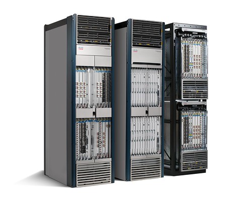
Advanced Platform Designed to Deliver New Wave of Video, Mobile and Data Center/Cloud Services
SAN JOSE, Calif., March 9, 2010 – Cisco today announced a major advancement in Internet networking - the Cisco® CRS-3 Carrier Routing System (CRS) - designed to serve as the foundation of the next-generation Internet and set the pace for the astonishing growth of video transmission, mobile devices and new online services through this decade and beyond.
With more than 12 times the traffic capacity of the nearest competing system, the Cisco CRS-3 is designed to transform the broadband communication and entertainment industry by accelerating the delivery of compelling new experiences for consumers, new revenue opportunities for service providers, and new ways to collaborate in the workplace.
Router Overview:
The Cisco CRS-3 triples the capacity of its predecessor, the Cisco CRS-1 Carrier Routing System, with up to 322 Terabits per second, which enables the entire printed collection of the Library of Congress to be downloaded in just over one second; every man, woman and child in China to make a video call, simultaneously; and every motion picture ever created to be streamed in less than four minutes.
The Cisco CRS-3 enables unified service delivery of Internet and cloud services with service intelligence spanning service provider Internet Protocol Next-Generation Networks (IP NGNs) and data center. The Cisco CRS-3 also provides unprecedented savings with investment protection for the nearly 5,000 Cisco CRS-1 deployed worldwide. Cisco's cumulative investment in the Cisco CRS family is $1.6 billion, further underscoring the company's commitment.
AT&T, one of the world's largest telecommunications companies, recently tested the Cisco CRS-3 in a successful completion of the world's first field trial of 100-Gigabit backbone network technology, which took place in AT&T's live network between New Orleans and Miami. The trial advances AT&T's development of the next generation of backbone network technology that will support the network requirements for the growing number of advanced services offered by AT&T to consumer and business customers, both fixed and mobile.
The Cisco CRS-3 is currently in field trials, and its pricing starts at $90,000 U.S.
Highlights and Capabilities for the Next-Generation Internet:
Unmatched Scale: With a proven multi-chassis architecture, the Cisco CRS-3 can deliver up to 322 tbps of capacity, more than tripling the 92 tbps capacity of the Cisco CRS-1 and representing more than 12 times the capacity of any other core router in the industry.
Unique Core and Data Center/Cloud Services Intelligence: In addition to capacity requirements, the growths of mobile and video applications are creating new multidirectional traffic patterns with the increasing emergence of the data center cloud. The new Cisco Data Center Services System provides tight linkages between the Cisco CRS-3, Cisco Nexus family and Cisco Unified Computing System (UCS) to enable unified service delivery of cloud services. This intelligence also includes carrier-grade IPv6 (CGv6) and core IP/MPLS technologies that permit new IP NGN architectural efficiencies required to keep pace with the rapidly growing cloud services market. Unique capabilities include:
Network Positioning System (NPS) -- provides Layers 3 to 7 application information for best path to content, improving consumer and business experiences while reducing costs.
Cloud virtual private network (VPN) for Infrastructure as a Service (IaaS)-enables 'pay-as-you-go' for compute, storage and network resources by automating Cisco CRS-3 and Cisco Nexus Inter-Data center connections for Cisco UCS.
Unprecedented Savings: The Cisco CRS-3 offers dramatic operational expense savings and up to 60 percent savings on power consumption compared to competitive platforms. The Cisco CRS-3 also delivers significant capital expenditures savings and investment protection for existing Cisco CRS-1 customers. The new capabilities in the platform can be achieved by reusing the existing chassis, route processors, fans and power systems with the addition of new line cards and fabric. These upgrades can be performed in-service and be provided by Cisco Services to ensure a smooth transition.
Silicon Innovation: The Cisco CRS-3 is powered by the new Cisco QuantumFlow Array Processor, which unifies the combined power of six chips to work as one, enabling unprecedented levels of service capabilities and processing power. Making this implementation even more unique is its ability to deliver capabilities with a fraction of the power required by lesser performing chipsets. The Cisco QuantumFlow Array chipset was designed to provide the new system the ability to scale with the ever increasing demands being placed on the IP NGN by the many different applications and billions of devices being used by both businesses and consumers in the Zettabyte era.
What ?.. People said!..
Keith Cambron, president and CEO, AT&T Labs
"We are entering the next stage of global communication and entertainment services and applications, which requires a new set of advanced Internet networking technologies. AT&T's network handled 40 percent more traffic in 2009 than it did in the previous year, and we continue to see this growth in 2010. Having leading edge experience in managing the largest global data network, we are pleased to continue our close working relationship with Cisco and its groundbreaking Cisco CRS-3 platform."
Pankaj Patel, senior vice president and general manager, Service Provider Business, Cisco
"The next generation Internet is upon us and we are confident that the Cisco CRS-3 will play a crucial role as service providers like AT&T deliver an exciting, new array of video, mobile, data center and cloud services. The Cisco CRS-3 is well positioned to carry on the tradition of the Cisco CRS-1, become the flagship router of the future and serves as the foundation for the world's most intelligent and advanced broadband networks."
Holding their ground on the PlayStation 3 update debate, hackers finally came up with a workaround for firmware v3.21. Sony's decision to remove support for installing other operating systems on PS3 consoles with their latest firmware update has been widely criticized, and left its users with the dilemma, update and lose this great feature or refuse the security updates and be unable to use PlayStation network (and hence online games).
George Hotz a.k.a GeoHot, promised just a few days ago that he would provide the Custom FirmWare for PlayStation 3 users who wishes to keep on using Linux flavours on their consoles with the existing 'Install Other OS' option. He pleaded for keeping the feature as is, and condemned such a move by Sony; also stating that he would find some method to safely update the firmware without loosing any of the existing features, if Sony sticks to their decision.
Seems like he proved yet again what he is capable of, demonstrating on a PS3 system. The custom firmware GeoHot labeled to be v3.21oo, runs flawlessly on a PlayStation 3 system, showing "System Software Version 3.21" as well as being able to boot into a Linux environment without a hitch. The custom firmware is only for the users running on v3.15 or prior firmware, and those who already updated their PS3 with Sony's v3.21 firmware are out of luck.
In his blog, GeoHot takes on Sony saying, all they are doing is to turn their 100000+ legit customers into hackers. He also expresses humorously that if he was someone who monetizes through his blog, he might have end up thanking Sony for taking this step, which increased the viewer traffic by 20 times. Though the CFW is already out to the mass, Sony is still completely silent regarding this whole event.
It seems as if the upcoming GameBone accessory and the gaming needs of thousands of iPhone and iPod Touch users have finally inspired Apple Inc. to develop a similar product, one that will allow users to operate their favourite Apple phone or media player with a variety of button-based controls, and give them the edge they’ve always wanted.
sneak peak on the patent application
Closer inspection however reveals that Apple filed this design, patent #0081505, in September 2008, and has been sitting on the concept for quite a while, way before GameBone detailed its own concept in June 2009.
The patent details various other functions and applications for the accessory, and it could contain force feedback actuators, accelerometer (for the iPod Touch), speakers, camera, microphone, even a mini keyboard, as well as infrared/Bluetooth wireless media controllers.
Check out the full patent and all its designs here [PDF] or here.
For those of us who thought the name Windows Phone 7 Series was too much of a mouthful, Microsoft has some deservedly good news: it will now be called Windows Phone 7. Period.
No more WP7S, no more Series…just WP7, and Windows Phone 7…much to the happiness of journalists, developers and involved users everywhere. The happily truncated name was announced on Microsoft’s Windows Phone official Twitter account, with the chirpy words: “Tis the season for Series finales. We've got one too - dropping the ‘Series’ and keeping the 'Windows Phone 7.' Done.” Talk about droppings on Twitter!
This move will not entail any technical changes, but is simply a change in branding.
All old enmities aside, Google has optimised many of its products for Apple’s latest game-changing device, the iPad.
The entire world seems to be cashing in on the iPad craze - with websites optimizing their pages, app developers creating specific new products or upgrading old iPhone ones, and video streaming sites resorting to HTML5 for iPad viewing - and Google is no exception.
The first of its products to be optimised is one of world’s favourite e-mail services, Gmail. While Google had already made a HTML5 iteration for Android and iPhone use, it has further customised the web app for the iPad by making it widescreen friendly, and providing the below pictured and quite handy 2-pane interface. It is to be used on iPad's native browser - Safari.
Other Google products optimised and available for the iPad include YouTube, StreetView, and GoogleMaps, apart from of course, GoogleSearch, which can be integrated directly onto the Safari browser (top-right corner). All these apps are available at Apple’s App Store, and many feature special gesture-based multi-touch controls. In related news, Yahoo has also launched a portal for the iPad, called Yahoo Entertainment.
Amidst the flurry of new open-source phone operating systems, such as Samsung’s Bada, Symbian^3, and Android, Intel and Nokia have finally released a pre-release build of their MeeGo, yesterday.
A Linux-based system, MeeGo is a developer-friendly combination of its parent’s previous operating systems, Moblin and Maemo, and will be released as a completely open-source operating system.
The pre-release build MeeGo OS source code is currently only compatible with the Nokia N900, Intel’s Atom line of computers, and Atom-based mobile phones. It currently is geared towards back-end development, and developer tools, with no GUI or front-end interface as yet. The OS code can also be booted from a USB flash drive, apart from the device directly. Imad Sousou of MeeGo describes the build, "The MeeGo common core includes the various key subsystems including the core operating system libraries, the comms and telephony services, internet and social networking services, visual services, media services, data management, device services, and personal services."
A full release of the OS code is due around May. 2010. Learn more and download the code at the MeeGo site.
Google is teaming up with Airtel to offer an ultra high-speed broadband Internet service in India. It looks like the 4Mbps connection for consumers and the 50Mbps broadband service for small businesses was just the tip of the iceberg, and Airtel has plans to cross a milestone in the Indian ISP business. If you recall, Google had already shared its plans to test an experimental gigabit network in the US. In this, India being behind the tech curve has proved to be of benefit, Google said, stating that India can leapfrog other countries which have to struggle with old lines and infrastructure. However, this won't be simple to implement and Google stated as much.
Airtel, meanwhile, has offered Google all the basic support, to reach out to the Indian metros, through their networks. Google thus needs to set up the TiSP Access Nodes and the central server, and Airtel will provide all the intermediate cabling and connectivity.
Airtel says, this service will be first available only in the major metropolitan cities of India; though no details on pricing has been announced.
Interested in using this 1Gbps line? Use this link to register yourself. The service will roll out on a first come, first serve basis, starting from next week.
Scientists at the University of Ohio have discovered what they claim to be the world’s smallest superconductor, which is less than 1nm in width. The superconductor works on a molecular scale and is formed by four pairs of molecules. The research was published in Nature’s Nanotechnology paper, and has been called a path-breaking idea in the field of nanoscale electronics.
In the past, interconnects of the modern chip fabrication process have always had problems with Joule heating and melting, as they traditionally have been built by metal, which conducts heat equally well as electricity. Interconnects on the nanoscale are called nanowires, whose electrical resistance unfortunately increases as they are made smaller.
have a look!.
However, using the new world’s smallest superconductor as the basis for a new-generation of nanowires might remove this problem altogether. Superconductors are so named because their electrical resistance tends towards zero, and will conduct electricity while only negligibly causing heat or power loss. The breakthrough comes with the fact that a certain superconductor is now known to be able to function on the molecular level, completely at odds with what scientists thought was a unshakeable truth, that superconductors only functioned on the macroscopic level.
These findings will have tremendous applications in nanoscale electronics, most notably in microprocessor design and fabrication.

 Found in an iPhone 3G case in a San Jose watering hole, the device has been observed to have a front-facing camera, a higher-res back-facing camera with flash, an 80GB hard drive, a 960x640 resolution screen, MicroSIM support, a “radio transparent” ceramic enclosure, and a “decidely new OS” which apparently does not boot anymore. Some seem to think this is device is still on a testbed frame, and that the final-release device will not have such visible and “un-Apple-like" seams on the side. The new owner is looking to sell the device. Find some more pictures in the gallery below.
 Images courtesy: Engadget and Weiphone